The photometric camera for the SDSS consists of two TDI scanning CCD arrays, one, using 30 Tektronix/SITe 2048 x 2048 CCDs in a 5 by 6 array for five-color photometry, and the other using 24 2048 x 400 chips for astrometry and focus monitoring. We here discuss these arrays, the filter system, the scheme for focusing the telescope during an imaging scan, and the CCDs and associated electronics for the camera and the spectrograph.
There are several important considerations in selecting the filter system. First, one wants the largest color baseline possible. It is desirable but not necessary to use filters for which there already exist a large amount of data. For example, the Thuan-Gunn (1976), (see also Schneider et al. 1983) uvgriz system, which has been used for much of the work at Palomar on distant clusters, avoids the 5577Å night sky line, and the i band cuts off in the near-infrared just shortward of the major OH bands. The g and r filters more-or-less match the J and F bands of the new Palomar Sky Survey. The uvgriz filters provide coverage of the total wavelength interval and are almost uniformly spaced in log lambda . They are, however, fairly narrow, and all except u could be usefully widened for a system like ours in which efficiency is of paramount importance. We have designed a filter system similar to ugriz which should transform to and from it with little difficulty, in which the g , r and i filters are as wide as practicable consistent with keeping the overlap small. If we wish the u band to be a "good" one which is almost entirely contained between the Balmer jump and the atmospheric cutoff (we can clearly not do anything about that end), it cannot be significantly wider than Thuan-Gunn u . We call the new system u' g' r' i' z' . The response curves and sensitivity data with the coatings and CCDs we will use are shown in Figure 8.1.
The SDSS system response curves. The responses are shown without atmospheric extinction (upper curves) and as modified by the extinction at 1.2 airmasses (lower curves). The curves represent expected total quantum efficiencies of the camera plus telescope on the sky.
The characteristics, are, in brief: u' , a band with 3540Å effective wavelength, 570Å full width at half-maximum, and 60% peak transmission (such a filter can be made with available glasses; it has a small redleak problem which can be solved with suitable coatings); g' , a very wide blue-green band centered on 4770Å (full width at half-maximum 1370Å); r' , a red band of the same width centered at 6230Å; i' , a far-red band centered at 7630Å with a width of 1530Å, and z' , a near-infrared band centered at 9130Å with a width of 950Å. These bands share the advantages of the uvgriz system of avoiding the 5577Å [OI] line, and the i' band cutting off before the catastrophic OH brightening and water absorption set in just longward of 9000Å. All the filters except u' are easy to make and have very high central transmission; building the u' filters proved to be difficult, but the results are quite satisfactory.
The filters are all made with one or more Schott colored glass elements in combination with a single-surface interference film which serves different purposes in different filters. The u' filter is made of 1 mm of UG11 and 1 mm of BG38 with an interference layer which both acts as an antireflection coating in the filter passband and an efficient red blocker in a region a few hundred Å wide around 7000 Å; the glass filters have sufficient red rejection outside this region, but the uncoated filter has a peak transmission of about two percent there. The coated filter has a maximum transmission of about 10-4 outside the primary band. The g' filter is made of 2 mm of GG400 and 3 mm of BG38, with a film which acts as a short-pass element cutting on at 5500 Å; the BG38 blocks the red efficiently out to the silicon limit. The three longer filters consist of a single colored long-pass element and for the two shorter ones a short-pass interference film, the r' 4 mm RG550 and short-pass cutoff at 7000 Å, the i' 4 mm RG695 and short-pass cutoff at 8500 Å, and the z' 4 mm of RG830 open to the red. Each filter is brought to 5 mm physical apex thickness by means of an (quartz for u' , BK7 for the rest) individual field flattener cemented to it; this element is necessitated by the fact that the chips are not flat, but are convex to the incoming light by about 230 microns measured center to corner. The final filters were all constructed and coated by Asahi Spectro-Optical in Tokyo; the characteristics and uniformity are superb.
The filter assemblies in turn are cemented to the flat rear face of the final corrector element. The front face of the corrector has been anti-reflection coated in horizontal stripes tailored for each filter passband, resulting in about 0.2% reflectivity over each band. The coating was done by QSP in Los Angeles. Since the filters are cemented assemblies and are themselves cemented to the corrector, there are only two optical surfaces near the CCD, and one of those has very low reflectivity. The other is the filter coating itself, which has low reflectivity in the passband but unfortunately has intrinsically high reflectivity near the long-wave cutoff over a very small wavelength region. It is these "crossover" regions which contribute most of the ghost energy. We have calculated ghost images for the camera, and they will not present a serious difficulty for the photometric reductions.
With our arrangement of CCDs operating in TDI mode at sidereal rate, we obtain near-simultaneous color data in the five bands; the time lapse from the r' data, the first received, to the g' , the last, is about five minutes.
It is worth noting that this color set is not any standard one, but this survey will produce two orders of magnitude more photometry than currently exists, and to adopt a system not optimized for the survey seemed folly. The filter set is in any case a good one for CCDs and has some quite nice astrophysical properties; we hope that it will quickly become a standard system. Toward that end we are in the process of producing as complete an astrophysical characterization of it (metallicity, gravity, temperature, galaxy type and redshift dependences) as we can; we clearly badly need these data ourselves. We will attempt to ensure that workers wanting sets of filters for this system will have reasonable avenues open to obtaining them.
With these filters, the CCDs with which they will be used, and with the SDSS telescope scanning at sidereal rate, the limiting magnitudes at the detection limit, S/N 5:1, will be about u'=22.3 , g'=23.3 , r'=23.1 , i'= 22.5 and z' = 20.8 . These limiting magnitudes are for stars, note, and those for galaxies are typically between half a magnitude and a magnitude brighter at the same signal to noise ratio. A signal to noise ratio of 50:1 (and hence photometry at the 2% level) is reached for stars at 19.3, 20.6, 20.4, 19.8 and 18.3 in the five bands. Note that these are magnitudes on the AB system, referred to a spectrum with constant fnu (not an A0V star), and represent the fluxes a flat spectrum source with a given V magnitude would have near the effective wavelengths of the filters. It is these zero points we intend to adopt. These sensitivity calculations assume 1 arcsecond FWHM seeing (with a probably somewhat pessimistic non-gaussian PSF) and a sky with a V surface brightness of 21.7 mag/arcsecond² (typical of the Apache Point site) with average extinction at the zenith. A darker site helps, with roughly half a magnitude gain in limit per magnitude improvement in the sky (at these faint levels shot noise in the sky is the dominant noise source).
Front view of the SDSS camera assembly. This diagram shows the camera as it would be seen with the front cover and shutters removed, showing the 30 photometric and 24 astrometric/focus CCDs and their associated dewars and kinematic supports.
Although the u' band is obviously useful, the other bandpasses provide a maximum wavelength ratio of 2.4, and adding u' only increases the baseline to 3.0. Is there much advantage to using u' versus a slightly longer wavelength band such as Johnson B or Thuan-Gunn v ? The answer is resoundingly yes, on three accounts. First, the u' -band is much more sensitive to population and metallicity effects than any of the longer wavelength bands. For example, for normal spiral galaxies, U-B changes 1.5 times as fast as B-V . In elliptical galaxies, color gradients (which most likely reflect metallicity variations) are 3 times as big in U-B as in B-V ; one must reach from B to the K -band to achieve comparable sensitivity. The u' -band lies shortward of the H and K break in late-type galaxy spectra and provides the best indicator of the presence of recent star-formation activity. Second, at high redshift, galaxies are usually observed in the more accessible and sensitive longer wavelength bands, which register light that, in the galaxy rest frame, is emitted in the ultraviolet. The u' -band is shifted to g' at z = 0.34 , r' at z = 0.83 , and i' at z = 1.3 . Third, the ultraviolet is essential in any color-based QSO survey to separate low-redshift ( z<2 ) QSOs from stars, particularly low-metallicity halo stars, and, incidentally, to separate low-metallicity halo stars from high-metallicity stars (cf. Figure 3.3.1.).
We had originally planned to devote two of the five chips in a given column to the u' band for the sake of efficiency, but new UV anti-reflection coatings and an accompanying surface treatment developed by Tektronix/SITe for the u' chips, together with a higher-than-expected efficiency of the u' filter, have led us to go with the current set of five independent bands, including the new z' filter. The new band is especially useful in the detection of very high-redshift quasars and extremely red stars, and, perhaps most importantly, distinguishing them from each other (see Section 3.3).
The photometric camera is designed to use thirty 2048² sensors in a six-wide by five-high array, so arranged that two transit swaths (strips) cover completely a stripe 2.53° wide in the five independent filters, with some overlap (about 1 arcminute) between sensors. About 8.3% of the area of a given stripe is imaged twice. The focal plane of the camera array is illustrated in Figure 8.2. Also shown there are the 22 smaller (2048 x 400) chips used to provide astrometric calibration, and the two 2048 x 400 focus monitors. The scanning is top-to-bottom in Figure 8.2, along the five closely-spaced CCD columns, and it is handy in discussing the camera to think about the geometry in this orientation. (Thus "top" of the camera will always refer to the leading edge.)
SDSS Filter Set and Photometric Sensitivity
| name | lambda | FWHM | qt | qtdl/l |
|---|---|---|---|---|
| u' | 3543 | 567 | 1.24x 10⁻¹ | 1.85x 10⁻² |
| g' | 4770 | 1387 | 4.51x 10⁻¹ | 1.18x 10⁻¹ |
| r' | 6231 | 1373 | 5.63x 10⁻¹ | 1.17x 10⁻¹ |
| i' | 7625 | 1526 | 5.02x 10⁻¹ | 8.74x 10⁻² |
| z' | 9134 | 950 | 1.29x 10⁻¹ | 2.23x 10⁻² |
| Filters | u' | g' | r' | i' | z' |
|---|---|---|---|---|---|
| Star saturates at AB | 12.1 | 14.1 | 14.1 | 13.8 | 12.3 |
| Eff Sky, mag/sec² | 22.1 | 21.8 | 21.2 | 20.3 | 18.6 |
| Sky + bkg count/pxl | 45 | 401 | 690 | 1190 | 1120 |
| Filter | u' | g' | r' | i' | z' | |||||
|---|---|---|---|---|---|---|---|---|---|---|
| AB | count | S/N | count | S/N | count | S/N | count | S/N | count | S/N |
| 17.0 | 32489 | 173.2 | 207754 | 442.2 | 206173 | 432.3 | 153488 | 352.8 | 32840 | 127.3 |
| 17.5 | 20499 | 134.6 | 131084 | 345.4 | 130086 | 334.4 | 96845 | 266.0 | 20721 | 88.8 |
| 18.0 | 12934 | 103.5 | 82708 | 267.4 | 82079 | 255.3 | 61105 | 196.4 | 13074 | 60.5 |
| 18.5 | 8161 | 78.4 | 52185 | 204.5 | 51788 | 191.6 | 38555 | 141.4 | 8249 | 40.3 |
| 19.0 | 5149 | 58.2 | 32927 | 153.7 | 32676 | 140.7 | 24326 | 99.3 | 5205 | 26.4 |
| 19.5 | 3249 | 42.2 | 20775 | 113.1 | 20617 | 100.7 | 15349 | 67.9 | 3284 | 17.1 |
| 20.0 | 2050 | 29.8 | 13108 | 81.2 | 13009 | 70.2 | 9684 | 45.4 | 2072 | 11.0 |
| 20.5 | 1293 | 20.5 | 8271 | 56.8 | 8208 | 47.8 | 6110 | 29.9 | 1307 | 7.0 |
| 21.0 | 816 | 13.8 | 5219 | 38.7 | 5179 | 31.8 | 3855 | 19.4 | 825 | 4.4 |
| 21.5 | 515 | 9.1 | 3293 | 25.8 | 3268 | 20.9 | 2433 | 12.5 | 520 | 2.8 |
| 22.0 | 325 | 5.9 | 2078 | 16.9 | 2062 | 13.5 | 1535 | 7.9 | 328 | 1.8 |
| 22.5 | 205 | 3.8 | 1311 | 11.0 | 1301 | 8.7 | 968 | 5.1 | 207 | 1.1 |
| 23.0 | 129 | 2.4 | 827 | 7.0 | 821 | 5.5 | 611 | 3.2 | 131 | 0.7 |
| 23.5 | 82 | 1.6 | 522 | 4.5 | 518 | 3.5 | 386 | 2.0 | 82 | 0.4 |
| 24.0 | 51 | 1.0 | 329 | 2.9 | 327 | 2.2 | 243 | 1.3 | 52 | 0.3 |
| 24.5 | 32 | 0.6 | 208 | 1.8 | 206 | 1.4 | 153 | 0.8 | 33 | 0.2 |
| 25.0 | 20 | 0.4 | 131 | 1.1 | 130 | 0.9 | 97 | 0.5 | 21 | 0.1 |
The expected photometric performance of the camera is outlined in Table 8.1, which presents the assumed filter parameters, derived from the curves in Figure 8.1. The quantity qt is the peak system quantum efficiency in the system, and qtdl/l is the integral of the system efficiency times d( ln lambda ) ; it is this quantity which relates the monochromatic flux averaged over the filter passband to the resulting signal:
The counts and signal-to-noise ratios for an assumed sky with a V brightness of 21.7 mag per square arcsecond (about 1.2 airmasses for the typical sky brightness at Apache Point) and a Palomar spectrum (Turnrose, 1974) are given in Table 8.1c for stellar objects with 1 arcsecond FWHM images with a reasonably realistic seeing-dominated PSF (see Chapter 13). The assumed exposure time is 55 seconds, which corresponds to a TDI scanning rate near sidereal; this rate is near optimal from a variety of considerations. The assumed full well is 3x 10⁵ electrons and the noise is a bit worse than typical at 7 e-. The assumed CCD quantum efficiencies are averages of the measured ones for the chips that will actually be in the camera; the dispersion is quite small. Typical galaxy images reach a given S/N half a magnitude to a magnitude brighter at the faint end, depending on their surface brightness.
Since the telescope has been designed carefully to accommodate the CCDs, the camera design is simply a matter of housing the chips stably, controlling their temperature, and tending to their various electronic needs. The only complication in this is brought about by the scale of the project and the attendant necessity of putting a lot of stuff, particularly circuitry, into a relatively small space. The only moving parts on the camera are associated with a simple set of pneumatically actuated shutters which cover each dewar and are intended mostly to protect the CCDs from saturation during the day and when the enclosure lights are on, though the shutter can also be used to take non-critically timed `snapshot' exposures. The camera will be installed and removed from the telescope with a special cart/handling fixture which also carries the "saddle" upon which are mounted a pair of 10-liter liquid nitrogen dewars and the power supplies for the camera. The camera is mounted to the telescope with a trefoil kinematic mount which is also shared with the plug-plate cartridges. The camera side of this mount is carried by a steel ring girder which provides the basic structure for the camera and a stable attachment point for the cell for the final corrector, which is the optical substrate upon which the sensors and filters are mounted, as will be described in greater detail below.
The CCDs for the photometric array will be housed in 6 long thin dewars (Figures 8.2 and 8.3) machined from aluminum blocks, each containing the 5 chips in one column. The CCDs are quiet enough to be run at -80°C, and will be kept at that temperature by an auto-fill liquid-nitrogen system which will be described in the next section. The optical system is fast enough and the focal plane big enough that mounting the chips and maintaining dimensional stability is potentially a very difficult problem. We seek to perform astrometry at the 30-milliarcsecond-per-coordinate level, which corresponds to 2 microns in a focal plane 600 mm in diameter. We have elected to solve this problem in a rather unusual but, we think, very satisfactory manner. The final corrector in the optical system is a quite thick piece of fused quartz with a flat rear face, 45 mm thick in the center and some 8 mm thicker at the rim, and we use this element as the mechanical substrate to which all the CCDs are registered and all the dewars attached. The corrector is thus both a mounting substrate and window for the camera dewars. Quartz is strong, reasonably stiff, has excellent dimensional stability and very small thermal expansion coefficient, and the small mechanical deflections associated with loading it with the camera have completely negligible impact on its optical performance. Figure 8.2 shows the front view of the whole assembly as it would look with the shutters removed, through the final corrector. Figure 8.4 shows the assembled corrector plate, mounted in its support, with the filters and the dewar mounting rails.
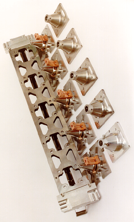
A disassembled photometric dewar. The CCDs are mounted on the invar optical bench (foreground).
The face plate (photometric corrector) of the photometric camera. The plate has been mounted in its steel cell. The filters from top to bottom are g' , z' , u' , i' , and r' . The astrometric r' filters are above and below the photometric array, though what is seen is the neutral density filters associated with those. The quartz kinematic mounts for the photometrics and invar ones for the astrometrics can be seen, as can the invar rails for mounting the dewar bodies and the screw anchors in the quartz for both. The boxes occupying the spaces the dewars normally reside in are just protective covers for handling.
The CCDs in the column are mounted 65 mm center-to center, which leaves 1.5 mm gaps between the 63 mm square Kovar packages in which the devices are mounted. There is a similar gap between the edges of the packages and the sidewalls of the dewars. The CCDs are individually cemented to the ball element of an invar-36 ball-and-socket mount whose center of curvature is at the surface of the chip (Figures 8.3, 8.5, and 8.7). These mounts provide tilt adjustment via a set of three push-push screws on each. These assemblies are in turn mounted on a `T'-shaped invar-36 optical bench (Figure 8.5) in a manner which allows small independent rotation of the chips and shimming for piston. The optical benches, one per CCD column, are mounted to the quartz corrector by a kinematic mount which consists of a quartz column bonded and screwed to the corrector, and a set of four ball-and-double-rod pads. On one end, the arrangement consists of two balls on sets of parallel ways, one parallel to the long axis of the bench and the other perpendicular, which locates that end in both dimensions to within small rotations. On the other, one ball rests in a set of parallel ways parallel to the bench, which fixes the rotation but is free to move along the bench, and the other in sets of mutually perpendicular ways, which is completely free to slide in the plane. The bench is sufficiently flexible in torsion that the four vertical constraints can be mated independently with quite reasonable dimensional tolerances and forces (50N) on the balls, and in fact needs the four-point support for torsional stability. The 3/16" balls are made of titanium, which is tough, combines reasonably good Young's modulus and reasonably low thermal conductivity, and the 3/32" rods of hard stainless steel. The conductive losses for each ball joint are about 0.5 watt, with the 100°C temperature drop shared roughly equally between the ball joint and the quartz pillar. We were quite amazed that the measured conductivity of the ball-rod joint was within about twenty percent of the calculated value for a wide variety of materials we tried; the scheme appears to work very well. The one disadvantage we know about for this scheme is that the stresses on the balls and rods are very high owing to the tiny contact area. There is no danger of failure at the static stress levels, but dynamic loading associated with handling could easily permanently deform either member. To avoid this, each dewar uses a set of four electroformed nickel bellows which are pressurized at 40 PSI to bring the optical benches into contact with the kinematic mounts for observing. When the camera is being mounted or otherwise moved, this pressure is relieved and springs retract the optical benches about 1 mm and latch them away from the kinematic mounts.
The optical benches (Figure 8.5) are quite stiff in bending. Loaded with their own mass and that of the CCDs with their ball-and-socket mounts their mass is about 2.7 kg and deflect about 1.3 µ in the focus direction and 1.0 µ in the focal plane under worst-case gravity loading. The kinematic mounts deflect a similar amount. Since the loading changes are very slow, the contribution to the astrometric error from these deflections should be negligible. The overall deflection of the corrector in the focus direction (which is the only direction there are appreciable deflections) is about 2 microns neglecting the stiffening by the dewar bodies. At worst focus changes induce centroid motion a factor of 20 smaller, so there is no appreciable error from this source. Since the dewars in this design are simply vacuum enclosures and, except for the preload bellows pushrods, do not even contact the optical benches, the load paths are very direct from the kinematic mounts to the telescope structure. The only tricky part of the design is the fact that there was a fair amount of (simple) machining to do on the quartz corrector. There are about 100 holes for screw anchors for the kinematic columns and the dewar mounting rails. The screw anchors consist of knurled brass inserts epoxied into these holes. The whole process went without mishap, though there was a fair amount of anxiety, as there was in applying the striped coatings.
Mounting the CCDs. The picture shows an invar optical bench, CCD mounts and the ball-and socket joints for tilt, rotation and focus of the CCDs. The copper contacts remove the heat load to the LN2 reservoirs via silver conducting straps. Note the setup of the kinematic mounting pins; the set in the upper left is the floating set, which mates with a pair at right angles on the quartz post.
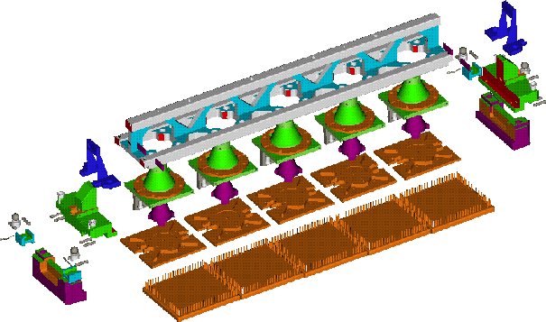
A CADD-generated exploded view of the optical bench assembly. The picture shows the bench, the kinematic mounts, and the CCD mountings. The ball mount which is cemented to the CCD package is itself a vacuum-brazed structure consisting of the stiffening plate (gold) and the ball (magenta).
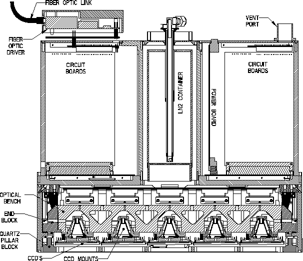
A central section side view of the photometric dewar. The locations of the liquid nitrogen reservoir and the electronics are shown.
It is, of course, necessary to adjust the tilt, rotation, and focus of each CCD fairly exquisitely; we allow 25 microns tilt error, 5 microns rotation error, and 25 microns total piston error. The tolerances on the absolute x,y location of the CCD are not severe, since there is no really significant software advantage to having objects centered on the same pixel on successive chips in the column and there is a 150-pixel overlap between successive TDI strips, but in fact the CCD assemblies and the machining and mounting of the optical benches has been done with sufficient precision that we expect the chips to be located within about 10 microns of their nominal positions. (We will not know for sure until the first TDI data on the sky is in hand). The tilt adjustment will be done on initial assembly of the ball and socket joint to theoretical optical design values. It can be changed on the basis of later tests but only with some difficulty; we feel, however, that it is the most reliable of the adjustments to predict. The rotation is much the most critical and will be done by the installation of a rigid lever on the socket part of the assembled ball and socket which extends some distance perpendicular to the optical bench. The optical bench will then be mounted accurately parallel to the ways of a precision linear slide and several reference points manufactured into the CCD which are exactly aligned with the CCD columns will then be examined with an inspection microscope as the optical bench assembly is moved along the slide. The rotational correction is then calculated and imposed by moving the lever with a micrometer screw. The lever arm translates the 5 micron tolerance over the 5 cm length of the CCD column to about 50 microns, which is easily resolved by the micrometer actuator. The socket must fit into the receiving hole in the optical bench to quite high precision, but the tolerances are not in fact very difficult with modern techniques, and were easily met in manufacture. Piston will be originally set with a set of shims to match the design focal plane. We expect to have to trim both the rotation and focus at the mountain, hopefully only once.
The dewar bodies themselves are machined of aluminum, and have O-ring seals to the quartz in front and to a fitted lid which carries the cooling system and electronics in back. They are about 75 mm tall and 330 mm long, so the atmospheric pressure on the sidewalls results in about 2500 N when they are evacuated. This is taken up by a lip on the lid of the dewar in back and in front by a frame machined integrally into the piece, which consists of horizontal bars between the filters. Thus the forces do not act on any dimensionally critical element. A similar force in the focus direction acts to seal the quartz to the dewar body, and demands that the face of dewar body be quite accurately flat in order that it not distort the rear surface of the corrector. This would have no optical consequence, but would change the effective shape of the focal plane. This strong bond with the dewars results in considerable stiffening of the corrector by the dewars, since the Young's moduli of aluminum alloys and quartz are similar; though the dewar walls are relatively thin (about 1 cm) they are twice as deep as the corrector is thick, and most of the stiffness is in the dewars. The great disparity of their thermal expansion coefficients, however, demands that the joint be a low-friction one; thin fluoropolymer gaskets appear adequate to the task. When the dewar is removed, fixtures attached to it bring the optical bench away with it for ease of maintenance. The optical bench can then be removed from the dewar through the top, carrying the in-dewar circuit boards (see Section 8.8 below) with it.
The dark currents for the Tek/SITe CCDs range from 30 to about 200 pA/cm² at 20°C. At -80 °C, this is reduced by about a factor of 3x10⁵, which for a 24 µ pixel becomes 0.01 electrons/second for 100 pA at room temperature. The sidereal-rate exposure time of 55 seconds thus yields a dark signal of about 5 electrons, which does not contribute significantly to the read noise. The total thermal losses for the dewar design we are using come to about 6 to 7 watts per dewar, three watts from radiation (mostly from the active detector area itself), 2 watts through the kinematic mounting, and another two from miscellaneous sources such as radiation to the nitrogen container, conductive losses through the flexible printed circuits (FPCs) connecting the CCDs to their support circuitry, conductive losses to the force actuators on the kinematic mounts, etc.
We will use an autofill LN2 cooling system patterned after the one used on the 4-shooter camera at Palomar (Gunn et al. 1987). Each dewar (Figure 8.7) will have a small LN2 container which holds about 200 ml of liquid, which will keep the detectors cool for about an hour. Under normal operating conditions all the LN2 dewars vent through a common vacuum-jacketed fill line and are kept under moderate pressure. There is a temperature sensor on the LN2 dewar body which is monitored continuously, and the dewar is filled when its temperature rises, but normally the dewars are filled on a schedule kept by the executive microprocessor (see below) which ensures that they never go empty. The fill is accomplished by opening all the solenoid valves on the individual vent lines and allowing liquid under pressure to enter; these are closed one by one as the dewars fill (as indicated by thermistor-based liquid sensors in the vent lines).
The heat is conducted from the chips through the kovar ball mounts cemented to them, and thence to copper posts which are connected via silver straps (silver is only slightly more conductive than copper but is nearly a factor of two more flexible at a given cross-section) to a cold-finger on the base of the LN2 container, which will also house a quantity of Zeolite molecular sieve getter. The very low heat conductivity of invar makes it difficult to keep the optical bench isothermal, but we will keep the chips at a uniform constant temperature with small make-up heaters associated with each CCD and mounted to the copper posts, as seen in Figure 8.5, which attach directly to the CCD mounts. The thermal expansion coefficient of invar is so small that small deviations from isothermality have little effect on the dimensional relationship in the bench. The temperatures will be measured with small platinum resistors fed with resistive dividers which result in reasonably accurately linear response over the relevant temperature range. Sensors of the same type are used to monitor the temperature of the LN2 container.
On the saddle which carries the power supplies (see below) are mounted two 10-liter intermediate supply dewars which supply the autofill system, each one supplying LN2 for one astrometric and three photometric dewars. These in turn are kept filled from a 160-liter dewar on the rotating floor of the enclosure, using an autofill system of rather different design.
It is necessary to do pretty good relative astrometry simply to place the fibers; with the other problems such as differential refraction with wavelength and position, hole placement uncertainties, etc, it seems necessary to find positions to accuracies of the order of 200 mas (12 microns in the focal plane) or so. This is difficult to do with the imaging array, because it saturates at about 14th magnitude in the bands useful for astrometry ( g' and r' , with r' preferred because of the smaller refraction corrections), and there are almost no astrometric standards at this brightness level. It would be in principle possible to calibrate the camera astrometrically, but one would have to depend on its stability and the stability of the telescope drives for relatively long periods to make use of the calibrations without suffering intolerable overheads. It would also be very nice from an astronomical point of view to do substantially better, and the astrometric CCDs illustrated in Figure 8.2 facilitate this.
They should allow tying the astrometric system of the survey eventually to the Hipparcos reference frame with an accuracy of order 30 mas locally, and if the survey could be redone in 10 years' time or so, would provide a wealth of proper motion data for faint sources. Even if there is no repeat, the utility provided by tying a faint QSO system to the Hipparcos one would be felt throughout astronomy. The astrometry is discussed more fully in Chapter 10 with respect to performance, Chapter 5 with respect to the survey strategy and in Chapter 3 with respect to scientific issues; here we address the hardware aspects.
It is a simple job to scale the existing 2048-square mask set to a nonsquare device with 2048 columns, so the astrometric CCDs are the same width as the photometric chips, but with fewer rows. A mask set for a 2048x 400 device was designed and produced by SITe, and two foundry runs of frontside devices made with it. We need a less tall device simply to fit into the available space above and below the photometric array, but there are other compelling reasons to favor such a geometry. We needed a number of these devices (24) comparable to the number of photometric chips, and it helped substantially that they were very much cheaper than the photometric CCDs; a device which is 2048 x 400 , which is the size we decided on, can be made several to a wafer, and is correspondingly cheaper than the one-to-a-wafer square device. Also, as we shall see, we require quite dense neutral filters to be able to observe available astrometric standards, and the smaller integration times associated with less tall chips allow us to use lower densities. The same consideration leads us to use less sensitive (by a factor of about 2) and much less expensive frontside illuminated CCDs. The disadvantage of the shorter columns is that the shorter integration times lead to larger position errors because of seeing-related image wander.
We have from these runs about thirty good devices. They have been mounted on precisely machined invar-36 headers of our design which allow the them to be mounted quite close together in the column (short) direction, as shown in Figure 8.2; the minimum distance is in fact determined by the necessary oversize of the filters to allow for the f/5 beam. The electrical signals to and from the chips are carried by flexible printed circuits of Kapton with very thin and narrow copper conductors. These FPCs are mounted permanently on the CCD headers and the chips are bonded out to pads on the FPCs.
For a chip 400 pixels high the integration time at the sidereal rate is about 11 seconds, and we argue in Chapter 10 that the one-dimensional positional accuracy achievable in that time is about 30-40 mas with the seeing conditions which must prevail during the imaging survey. These chips can be run somewhat warmer than the photometric imaging devices because we are not interested in low signal-to-noise objects and the integration time is short. Cooling to -60 °C is sufficient, which yields a background of about 10-20 electrons per pixel in the 11 second integration time for these devices. The centroid of a star which deposits about 2000 electrons can be measured to about 30 mas (shot and readout noise errors alone) in 1 arcsecond seeing with this background. A star which saturates in the central pixel ( 4 x 10⁵e- for these devices) has a total signal of about 4x 10⁶ electrons, so the dynamic range for 30 mas accuracy, considering shot and read noise alone, is about 8.3 magnitudes.
We will use the astrometric sensors in the r' band, which seems optimum. With no further attenuation, they will saturate at about 11.3, and one can do 30 mas astrometry to about 19.5. This is not particularly useful, since the Hipparcos net and the AGK3 have very few objects as faint as 11.3. We will use 3.0 magnitude neutral filters, for a useful range of 8.3 to 16.5 This filtration results in an overlap of about 2.5 magnitudes between saturation of the imaging array (about 14.0), and the 30 mas accuracy limit for the astrometric array, and there are more than 200 stars per square degree in that magnitude interval near the pole. Thus the frame defined by the astrometric chips and the one defined by the red imaging chips (and with only a little more difficulty, that defined by any band in the imaging array) can be tied together very accurately indeed. Most of the Hipparcos stars are fainter than 7th, so more dynamic range would not really be useful.
We will use a total of 24 of these devices, one at each end of each column of photometric CCDs, 5 across the top and bottom of the array to tie the columns together, and two outside these to provide focus information. The sensors at the bottom provide a check on the tracking rate and direction; stars cross the bottom set 7.5 minutes after they cross the top, and they go through the red photometric sensors at 1.4 minutes. Thus drive errors with frequencies lower than 2 x 10⁻³ Hz can be corrected for, and we can monitor higher frequencies statistically. The astrometric and red sensors define a continuous frame which will drift slowly with respect to any initially defined absolute frame because we are basically measuring rates. We will use the astrometric standards only to pin this instrumental frame to the sky at intervals (see Chapter 10).
There are about 1.5 Hipparcos stars per square degree in our magnitude interval, and the array will encounter one every 70 seconds on average. If the drives can be held to the accuracy we would like (25 mas rms stochastic component in the frequency interval 2x 10⁻³ to 3x 10⁻¹ Hz), as seems very likely from measured errors on the manufactured parts, tying the survey to the Hipparcos net to 30 mas should be possible; in any case, we should be limited to the errors imposed by seeing, which is our goal.
The dimensional relationship between front and rear ranks of the astrometrics is also crucial to control, since that determines the accuracy with which errors in the drive rate and direction can be measured. This is greatly facilitated by our use of the quartz corrector as the metering substrate, and the dimensions should not be much less accurately maintained than those within one of the optical benches, particularly when one considers that the deflections associated with the kinematic mounts are the same for the front and rear benches (and furthermore quite similar to those for the photometric benches).
At an operating temperature of -60 °C the total heat load to the astrometric optical bench is about 6 watts, roughly the same as the photometric dewars. We have decided for simplicity and economy to use a cooling system essentially identical to the one adopted for the photometric dewars, and in fact one which shares many parts with its photometric counterpart. In this case we must endeavor to keep the bench as isothermal as possible. The bench has a cross-section of about 7 cm², and the conductivity of invar is about 0.2 watt/°C-cm, so a flux of 1 watt in the bench is associated with a temperature gradient of about 0.7° per cm. Temperature differences across the bench of 1 °C induce a bow in the bench with an amplitude of about 1µ. We will distribute the heat load from the bench to a heavy cold bar attached to the LN2 container's coldfinger at four points along the optical bench, again using thin silver straps. This will result in temperature inhomogeneities of the order of 1 degree, but in a pattern which should remain quite stable and hence innocuous astrometrically.
It is clear that one of the major contributions to image degradation in normal observing circumstances is the inability to keep up with focus changes brought about by flexure and temperature changes, and we will address this problem at the outset. Our requirements are especially severe because of the astrometry, but it appears that a simple scheme will suffice to provide excellent control.
There are two astrometric-type sensors housed in the astrometric dewars which will be used as focus sensors; though they are quite far from the center, the image quality is quite good at their location. They will have only an r' filter with no neutral density; this filter is cut into three parts, and the optical thickness associated with the neutral filter on the other sensors is taken up by three clear glass spacers of varying thickness. When the the rest of the array is in focus, the center of the focus chip is also, but the ends are, respectively, 300 microns inside and outside of focus; this defocus, which results in image degradation from defocus comparable to the expected 1 arcsecond seeing, is optimal from a focus-determination signal-to-noise point of view. Comparison of the images in the two outer thirds will provide a sensitive differential measure of the focus, which we will adjust dynamically; the resolution of the secondary motion is such that that should cause us no difficulty. Figure 8.8 shows images at five positions on the focus sensor through focus with 150 µ focus steps, as produced by the design optical system and convolved with 0.8-arcsecond Gaussian seeing.
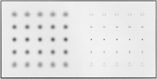
Focusing the camera. Images in the focus CCDs are shown at at five positions across the chip and at focal positions -300 µ, -150 µ, 0, +150 µ, and +300 µ referred to best focus. The left panel are the images as produced by the telescope, the right convolved with 0.8 arcsecond Gaussian seeing.
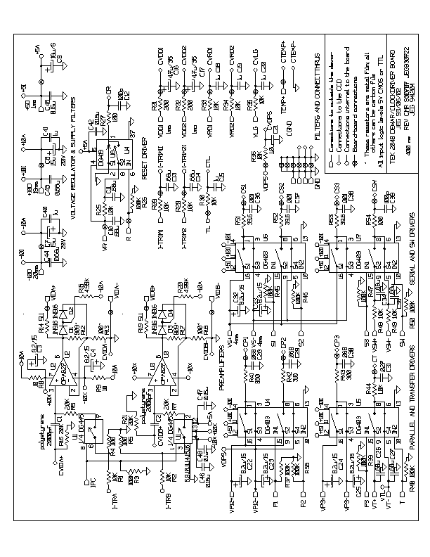
Schematic of the in-dewar electronics. Included are the dual preamplifier and the CCD clock drivers. This is implemented as two small piggybacked surface-mount cards which are mounted on the dewar wall.
Each CCD is associated with either one or two analog signal chain channels; the Tek/SITe chips have split serial registers and we originally hoped that we would be able to obtain all our devices with two good amplifiers on at least one of the serial registers. This would have allowed us to use rather slow readout, with correspondingly good noise performance. As it turned out, it was expedient to accept a small number of devices (6) with only one good amplifier, which we have to run twice as fast. The noise penalty is only about a factor of 1.3, and in most cases is not a serious problem. We strongly considered running all of the devices with one amplifier, but unfortunately not all the devices will run fast enough. Thus the electronics is not quite synchronous, there being two serial clocking schemes, one running exactly twice as fast as the other but both generated from a single master clock and locked in phase.
The architecture of the serial registers on the devices is such that there are 20 `extended' pixels between the edge of the imaging array and the on-chip source follower amplifier, and we will read another 20 overscan pixels in the two-amplifier chips, so each half-row will consist of 1024 + 20 + 20 = 1064 pixels. The single-amplifier chips will have the 20 leading and trailing extended pixels at either end of the data pixels and will in addition have 40 overscan pixels at the end. At sidereal scanning rate, the scale of 3.643mm/arcminute corresponds to 38.05 lines/sec, or 26.28 ms/line. The vertical transfers require about 700 µs, leaving 25.58 ms per line. At 24 µs per pixel, the time for 1064 pixels is 25.54 ms. (The fast channels run at 12 µs per pixel, clearly.) We need about 32 master clock cycles per pixel for all the functions in a classical dual-slope double-correlated sampling system, so a 1.3333 MHz (750 ns) clock yields 24-microsecond pixels. This will be derived from an 8 MHz master clock, which is needed by the A/D converters and the data transmitters.
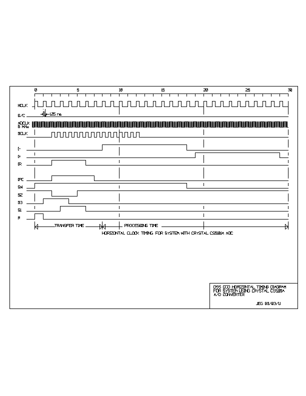
Timing and CCD control. The figure shows the timing diagram for the horizontal charge transfer, double-correlated sampling control, and analog-to-digital conversion for one channel of a double-amplifier chip. The pixel clock is 1.3333 MHz, derived from the 8 MHz master clock which also runs the internal conversion circuitry on the Crystal CS5101A converter.
A schematic of the dual signal chain and A/D board.
There is some question about whether 16 bits is enough (probably academic, since at the moment more accurate converters in this speed range are not readily available), but the problem is not severe. In the g' , r' , and i' bands the sky levels are such that digitizing at roughly 5 electrons/(AD unit) results in a step which is small compared to the standard deviation in the background, and accommodates with 16 bits the full 300,000 electron full well of the device. In the u' chips the situation is not quite so good. The sky in each chip is only of order 50 electrons, and the noise with 5 electrons read noise per chip is 9. If we demand that we digitize at at least two levels per unit sigma, this will result in a digital full well of slightly less than the physical full well of the CCD. This is not a serious problem, however, since the fluxes and efficiencies are such that no object which does not saturate in one of the other bands is likely to overflow the u' A/D.
The CCD voltages and the voltages required to trim the dual-slope circuitry are generated by a set of three octal 8-bit DACs, Maxim 528s, for each chip. These converters have serial input, and all the converters in the system are daisy-chained to be set up with one very long serial word. The output voltages are sampled and placed on an output bus for measurement with a set of serial-input 8-position analog switches. The circuit for this voltage generator and monitor is shown in Figure 8.12. The signal chain electronics and this circuit are implemented in surface-mount technology on opposite sides of one small 8-layer Eurocard, all of which again have been constructed and tested. There is one of these cards per chip on the photometric camera. Some of these cards, associated with the single-amplifier chips, use only one signal channel, but all the cards are identical except for the input resistors which are used to trim the gains to match the individual output amplifier gains for each CCD, and the integrator capacitor, which is a different value for the fast single-amplifier circuitry. Thus each photometric dewar contains 5 of these cards, plus one card which is basically a bus receiver for the clock signals described in the next paragraph; the astrometrics employ 6 plus a bus receiver; all of the astrometric chips run with only one amplifier to save cards and space, and so we run two chips with each signal-chain-bias card -- the performance penalty is negligible.
A schematic for the voltage generator board for the SDSS cameras. All the voltages are generated by DACs and the board also has provision for placing any voltage on a measurement bus for monitoring.
The clock signals are generated from programs stored in EPROMs and controlled by a Forth microcontroller using a Hitachi H8/532 CPU from Triangle Data Systems. One controller runs the entire camera; all CCDs are clocked synchronously with identical clocking waveforms (though there are two sets of serial waveforms for the `fast' and `slow' chips.) The voltage rails for all voltages can be optimized for each chip. The controller has two such CPUs, one of which is busy continuously generating the CCD signals, and the other of which (the `executive') is keeping track of other housekeeping chores, such as control of the shutters, initial DAC voltage setup, voltage and temperature monitoring (the micro has an on-chip 10-bit A/D), etc. We monitor all the operating voltages (the CCD temperatures are part of this set) on a round-robin basis, measuring one voltage per line time. There are 22 voltages for each of 54 CCDs, so the process requires about 32 seconds for one cycle. The ADC setting requires a word a little more than 10000 bits long, which will have a leading checkbyte which is received back at the transmitter after making the entire rounds. The clock will be slow, 10kHz, and so the setup time is 1 second. All signals are sent from the controller by balanced RS485 transmitters and received at each dewar by complementary receivers. All signals except the 8 MHz master clock are carried on a 100-conductor ribbon cable bus. The control for the camera comes over a single `RS232' fiber pair to the executive micro. There is considerable flexibility for controlling the chips with this scheme; we implement on-chip binning both horizontally and vertically (independently) and allow some control of the sampling interval. There is, in particular, a "quick" mode in which the CCD clocking is identical to that usually employed but which cuts the sampling time by a factor of five. This allows the chips to be read at twice the usual speed with a noise penalty of a factor of 2.3, which is useful for calibration exposures for the spectrographs (this mode cannot be used for the camera, because the single- channel chips cannot be run this quickly owing to the limitations of the ADCs). We will also have the capability to bin very heavily vertically, which will be used in spectrophotometric calibration for the spectrographs.
The Crystal A/Ds have a serial output, which is fed (again over RS485) to a pair of small cards mounted piggyback on the dewars which carry RS485 receivers, circuitry to format the data for the single-channel chips to resemble that for the dual-channel chips (in the time domain), a programmable logic chip which acts as a serial-to-parallel converter and multiplexer, and a fiber-optic FOXI transmitter to send the data to the DA system in the operations building. Each of these cards is capable of handing 12 slow data channels or 6 fast ones or any admixture. Each photometric dewar has one and each astrometric dewar 2, for a total of 10 data fibers for the 10 DA computers (see Chapter 14).
Each voltage-generator/signal chain card dissipates 2.8 W, the bus receiver and a voltage regulator-voltage distribution board about a watt each, so the photometric dewars dissipate about 16 watts each and the astrometrics about 20 watts. This waste heat is handled by the cooling system for the telescope. The camera enclosure acts as a semi-sealed chamber in which air is both generally circulated and blown specifically into the electronic enclosures associated with each dewar; the heat exchanged into the air is removed with two liquid-cooled heat exchangers on the fans. Water-glycol is provided to these exchangers at about two degrees below ambient, the goal being to keep the camera enclosure at ambient temperature. A similar scheme is used in the camera power supplies.
The power supplies are not mounted directly with the camera but are carried on a separate "saddle" which is mounted with, travels with, and is dismounted with the camera but is mounted to both the cart and the telescope mechanically and thermally independently. The saddle also carries two ten-liter intermediate "holding" dewars which supply LN2 to the small-capacity LN2 containers associated with each CCD dewar. Each dewar has its own power supply, each of which is implemented using small encapsulated linear supplies on a single 20x25 cm printed-circuit card. Each supply carries a fairly sophisticated monitoring and shutdown system mounted on a separate smaller PC card. The supplies are packaged in two identical chassis, each set serving one astrometric and three photometric dewars. There is in each chassis also an "auxiliary" supply to run the control micros, the LN2 system, the fans, solenoid valves, etc.
Thus the camera has a power cable which is made up of ten identical dewar power cables, an RS232 fiber pair, and ten data fibers as electrical connections to the outside world. It has in addition cooling water/glycol, a single vacuum-jacketed LN2 supply, pressurized N2 for the shutters, and pressurized N2 and vacuum for the dewar kinematic mount force actuators.
Identical analog electronics are used on the spectrographs; there there will be a controller per spectrograph, so each spectrograph has a data fiber, and since those CCDs are not used in TDI mode, there is no need for an executive micro. The spectrograph dewars are copies of the Palomar 4-shooter dewars and will employ the same autofill system as the photometric camera.
This whole project hinged quite visibly on the availability of many (42, including spares) 2048 x 2048 CCD sensors, at least 8 of which need excellent UV sensitivity and very low readout noise ( < 5 electrons.) At the inception of the work which has led to this proposal more than ten years ago, it was by no means obvious that the chips could be obtainable. The project is really not viable in anything like its present conception without them, and though quite powerful surveys could be pursued with smaller detectors, we would either have given up a great deal which we believe is vital, have been stuck with an impossibly complex system (would you really like to align a focal plane with 120 1024 x 1024 CCDs and tend to their electronics?) or extend the survey time-to-completion unconscionably.
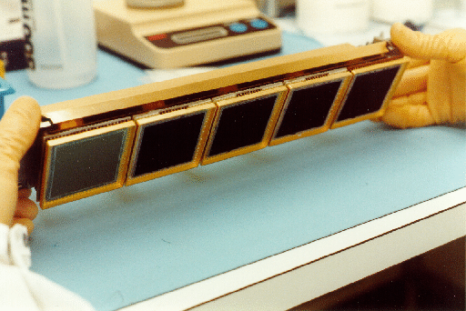
Five CCDs on an optical bench, with the gold plated heat shield in place.
The situation improved very markedly in the intervening years. Tektronix produced large numbers of 2048 x 2048 21-micron pixel devices as part of NASA's STIS program for the second-generation Hubble Space Telescope instrumentation, and went on to produced for our project a foundry run of excellent 24-micron devices, from which we were delivered 5 working and two excellent chips. Subsequent to that, we negotiated a contract for all the chips for the survey, photometric and astrometric/focus, with SITe, the now-independent Tektronix CCD division. Our cosmetic requirements are quite different from most of SITe's customers, since TDI gets rid of a whole suite of defects which would mar performance in normal imaging mode, and they agreed to deliver chips with special grading for us at a price somewhat below that for their normal Grade 1 devices. This arrangement was spectacularly successful, and we now have in hand and have fully characterized all the chips for the project (including the camera, the Monitor Telescope, and the spectrographs) including spares. Five CCDs, mounted on their optical bench, are shown in Figure 8.13. This picture shows the CCD complement for one of the six photometric dewars.
The charge-transfer problems which plagued the early large devices were solved and considerable progress made toward effective antireflection coatings and backside treatment for high stable quantum efficiencies in the blue and near ultraviolet. The engineers at SITe pursued two paths toward ultraviolet sensitivity; one of implantation techniques to keep the backside properly charged, and the other of coatings to reduce the severe reflection losses in the blue and near UV. They have consistently produced chips with better than 50% QE at 3500 Å. The quantum efficiency for thinned CCDs with the "standard" and the delivered UV AR coating are shown in Figure 8.14. One disappointment we have had is that this high UV QE declines substantially at low (operating) temperatures, but still is in the vicinity of 40% for all our devices at -80 °C at 3500 Å.
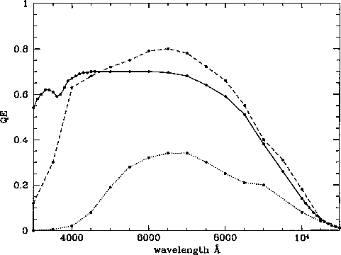
Quantum efficiency curves. Data are shown for the standard AR coating (dashed) and for the new UV AR coating (solid) on thinned SITE CCDs. The QE for the unthinned chips (dotted) is shown also for comparison.
The new chips have many of the latest `wrinkles'; there is a mini-channel in the columns for very good low-level charge transfer efficiency, the chips can be run in MPP mode (not, unfortunately, in the scanning array, since they are clocking all the time), and have amplifiers with very small geometry for the lowest possible noise.
The chips are designed and bonded out so that the four quadrants can be read independently, which for many applications results in a factor of 4 improvement in readout time; for us, it is the split in the serial direction which is useful, since we must integrate over the full chip vertically. It would be well to have all four amplifiers working for the spectroscopic chips, but that is sadly not the case for the chips in hand. The readout time for a two-amplifier chip is about 1 minute, or 30 seconds in the higher-noise `quick' mode, which can be used for spectroscopic flat fields and wavelength calibrations.
The devices were first characterized roughly at SITe and sent to Princeton for final evaluation. We have a cold test station which is controlled by a 486 PC which has electronics similar to the survey electronics. The system noise is about 1 electron, and we have the capability to measure CTE, quantum efficiency as a function of wavelength, uniformity, and also to test the vertical CTE in TDI mode using a special parallel-bar target and a flashlamp. The technique involves running the chip for some time with a uniform "sky" background of appropriate level, and then exposing the bar target, which consists of about 200 thin bright lines parallel to the rows of the CCD, with a flashlamp to impose a low-level signal. This frame of data is then captured as the chip continues to scan in TDI mode, and the bars are superposed to simulate a single such bar traveling along the chip following the charge packets. Doing this is important, because some low-level parallel traps which show up in single frames are satiated by the sky in TDI mode and disappear; other stronger traps permanently damage the CTE in the affected columns.
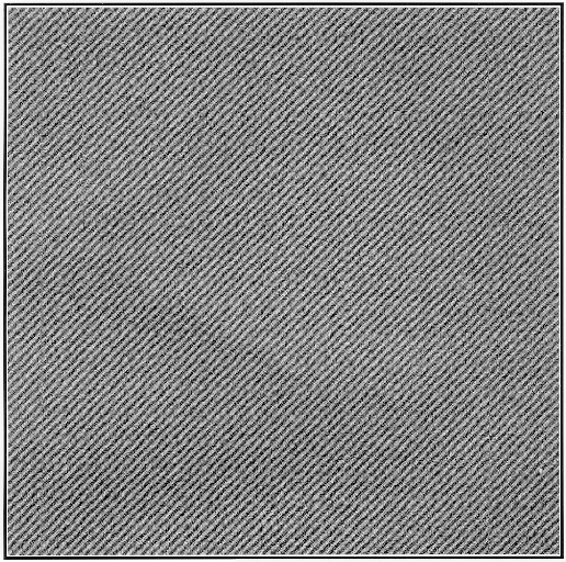
A subimage taken from a typical survey-grade CCD. The target is a 45° Ronchi ruling with a half-pitch of 3 pixels perpendicular to the rulings. The image has 30 electrons in the white bars, less than 3 in the black ones.
Our specifications allowed for single bad columns, the notion being that we are well-enough sampled that we can effectively interpolate across one bad column, but two or more contiguous ones disqualify a device from our consideration. Interpolation does, of course, affect the statistical accuracy of the photometry of objects affected by the column, but that is easy to keep track of and account for in the data reduction. The spectroscopic chips will be arranged so that the spectra are along columns, because the defects in CCDs are almost always along columns; thus even catastrophic column defects simply wipe out the spectra from a few fibers which we know about and can simply avoid using, and we have so many. Here, unlike the situation with the imaging array, we prefer for a given number of defects for them to be grouped, though here again the loss of a single column in a spectrum is not necessarily a disaster. This is but one example of our special requirements.
Partial blocked columns, for example, show up in TDI as columns with stably depressed quantum efficiency, and if the fraction of the column blocked is not too large has almost no effect. Likewise single hot column defects are integrated over and can be simply subtracted out if the noise contribution is not too great or interpolated over if it is.
Our chips all have good to excellent electrical performance, with amplifier noise varying between 2.5 and 10 electrons for all devices accepted for use in the three bluest bands, and a few with noise as high as 20 for the i' and z' bands, where the sky background will be about 1000 electrons per pixel. The median noise is near 5 electrons, and we measure CTEs of around 0.99998 horizontally and 0.99994 vertically at illumination levels of 30 electrons. This improves to about 0.999993 horizontally and 0.99998 vertically at 300 electrons, which is typical of all the expected backgrounds except for the ultraviolet. At the lower level, which is somewhat less than the ultraviolet sky level, the net transfer efficiency is 86 percent from the upper center of the chip (the pixel with the largest number of transfers). This represents a shift of 0.02 pixel horizontally and 0.07 pixel vertically (averaging over the column as TDI does) and completely negligible PSF degradation. For the higher-background chips these numbers are more like 0.007 pixel horizontally and .02 pixel vertically. The overall cosmetic uniformity is excellent as well, with RMS large-scale QE variations of about 7% in the blue and 4% in the red and infrared. The main defects we have seen are parallel traps of various strengths, many of which are strong enough to cause serious CTE degradation in the vertical direction with the backgrounds we are using, though again they are not fatal if they involve only one column. A subimage in the corner farthest from the amplifier taken with a quite typical device of a ronchi target with 30 electrons signal in the bright bars is shown in Figure 8.15, in which the excellent cosmetics and low-level CTE is seen.
We elected to take chips mounted in their standard kovar packages even though this led to significant mechanical difficulty in their mounting and cooling; demanding better packaging would have precluded culling our devices from a commercial production stream and would have prohibitively increased the cost. The problems incurred are fairly serious, however. The expansion coefficient of kovar matches silicon (and the substrate for the thinned devices, which does match silicon well) so poorly that the overall curvature of the devices, already serious at room temperature because of problems in high-temperature processing, is much worse at operating temperature. As mentioned above, the chips are convex toward the incoming light by about 230 microns center to corner, and that value roughly doubles cooling to -80 C. We have dealt with this both for the spectroscopic and photometric chips by cementing a heavy kovar stiffener to the back; in the case of the photometric chips, this is part of the ball tilt mounting. It was also necessary to build a precision measuring microscope to aid in the gluing of the photometric chips, since we wished to position the chips to pixel-or-subpixel accuracy and the chips are not mounted very accurately in their headers. We thus used reference points on the die itself to reference the CCD to its ball mount, and succeeded in doing so to an accuracy of about 3 microns RMS.
Our requirements for spectral sensitivity and noise vary a great deal across the array, though for the u' chips (7 with spares; we have spared the equivalent of a complete 5-chip dewar) we certainly require both good UV sensitivity and very low noise. The original requirements we imposed are summarized in Table 8.2. The chips we have received and will use are better than these specs in most respects. The operating temperature quantum efficiencies are well exceeded in all devices except those for the u' band; the mean qe for the z' chips is 14 %; for the i' , 60%; for the r' , 78%; for the g' , 70%; and for the u' , 38%; the dispersions in these numbers are small and probably dominated by measuring error. We have built in to the dewars UV floodlamps and can use them to enhance the UV quantum efficiencies to approximately the spec 45%, but whether we will use them or not is a complex operational issue, since the effects of UV flooding are not permanent and there is a significant dark current penalty. The noise specs are also all met except for the u' , where the worst figure is 6.4 electrons.
It goes almost without saying that the development of these devices for the survey has had tangible benefits for all of optical astronomy. Though the major thrust of wafer-scale large CCDs has now gone toward devices with more but smaller pixels resulting in slightly smaller devices overall, the production of these chips with high yield depends heavily on techniques learned here.
Gunn, J. E. and Westphal, J. A. 1981, Proc SPIE 290, 16.
Gunn, J. E., Carr, M., Danielson, G. E., Lorenz, E. O., Lucinio, R., Nenow, V. E., Smith, J. D., and Westphal, J. A. 1987, Optical Engineering, 26, 779.
Gunn, J. E. 1989, in Clusters of Galaxies, W. Oegerle, M. Fitchett, and L. Danly eds., proceedings of the third Space Telescope Symposium, Cambridge, 341.
Schneider D. P., Schmidt, M., and Gunn, J. E., 1989, A. J. 98, 1951.
Turnrose, B. 1974, P. A. S. P. 86, 545.